News Story
Professor Aristos Christou Leads Research of Diamond Electronics

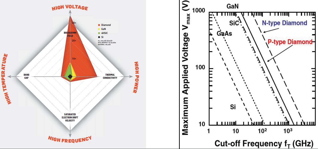
Figure 1 (left): Comparison of physical properties of diamond (orange) with GaN (yellow), SiC (green) and Si (black). All values scaled with respect of silicon material values. Figure 2 (right): Performance limits for applied voltage and cut-off frequency for diamond, in comparison to GaN, SiC, GaAs, and Si.
Since the loss of the Telstar I satellite in 1962 after a high altitude nuclear test, it is known that radiation may perturb the operation of electronic equipment. Radiation hardened semiconductor devices are essential for defense electronics, surveillance satellites, microwave and millimeter wave communication, instrumentation for nuclear power plants, and detectors for high-energy physics experiments. Now Wide band gap Semiconductors have become essential for smart grids, high power converters and power electronics for wind turbines.
MSE Professor Christou’s research will develop Diamond for DoD-critical power RF electronic devices due to its exceptional physical and electrical properties such as higher breakdown voltage (>10 MV/cm), high hole carrier volume mobility (>3800 cm2/V·sec), extremely high thermal conductivity (>22 W/cm·K), and excellent mechanical and thermal stability in vacuum. The Defense Threat Reduction Agency has selected Christou to lead the effort for revolutionizing Diamond Electronics. Why diamond and not some other semiconductor material? The exceptional properties of diamond are summarized in Figure 1, while Figure 2 shows that performance limits for diamond clearly exceeds the limits for SiC and GaAs. In addition, diamond offers a greater inherent radiation hardness from the start, an advantage over various power SiC and GaN devices with known problematic radiation effects. Diamond as a semiconductor has fundamental advantages and issues which to the present have not been resolved. The known doping elements (B, P, Si and N) form deep centers, which create low carrier concentrations at room temperature. At high boron doping concentration, diamond becomes semi-metallic but its mobility substantially drops. Therefore, devices based on bulk transport in diamond result in either low mobility or low free carrier concentration at room temperature.
Dr. Christou’s research is to overcome these problems through a hydrogen terminated surface, which has a negative electron affinity resulting in the establishment of a two-dimensional hole gas (2DHG) transport layer just below the surface. The 2DHG layer has both high carrier mobility and high carrier concentration. The surface-conduction layer gives rise to a p-type surface conductivity with a hole mobility of typically 100-200 cm2/V·sec and channel sheet hole concentration of 1012-1013 cm-2. Innovative microwave power field effect transistors (FETs) with the diamond surface conduction channel with cutoff frequencies above 50 GHz and power gains of over 1 Watt/mm have already been demonstrated and Professor Christou is to further improve these limits and ensure that these new devices can resist exposure to radiation.
Published December 1, 2016


