News Story
Salamanca-Riba Silicon Carbide Research Highlighted by NIST

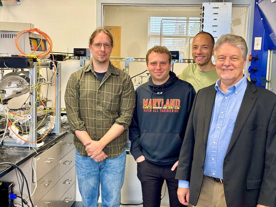
Professor Lourdes Salamanca-Riba.
The article, titled "University-Army Collaboration Investing SiC-based MOSFET Treatments," describes a collaboration among researchers at the University of Maryland, Auburn University, and the Army Research Laboratory. The team is investigating performance and reliability-enhancing treatments for silicon carbide (SiC)-based devices used in communications.
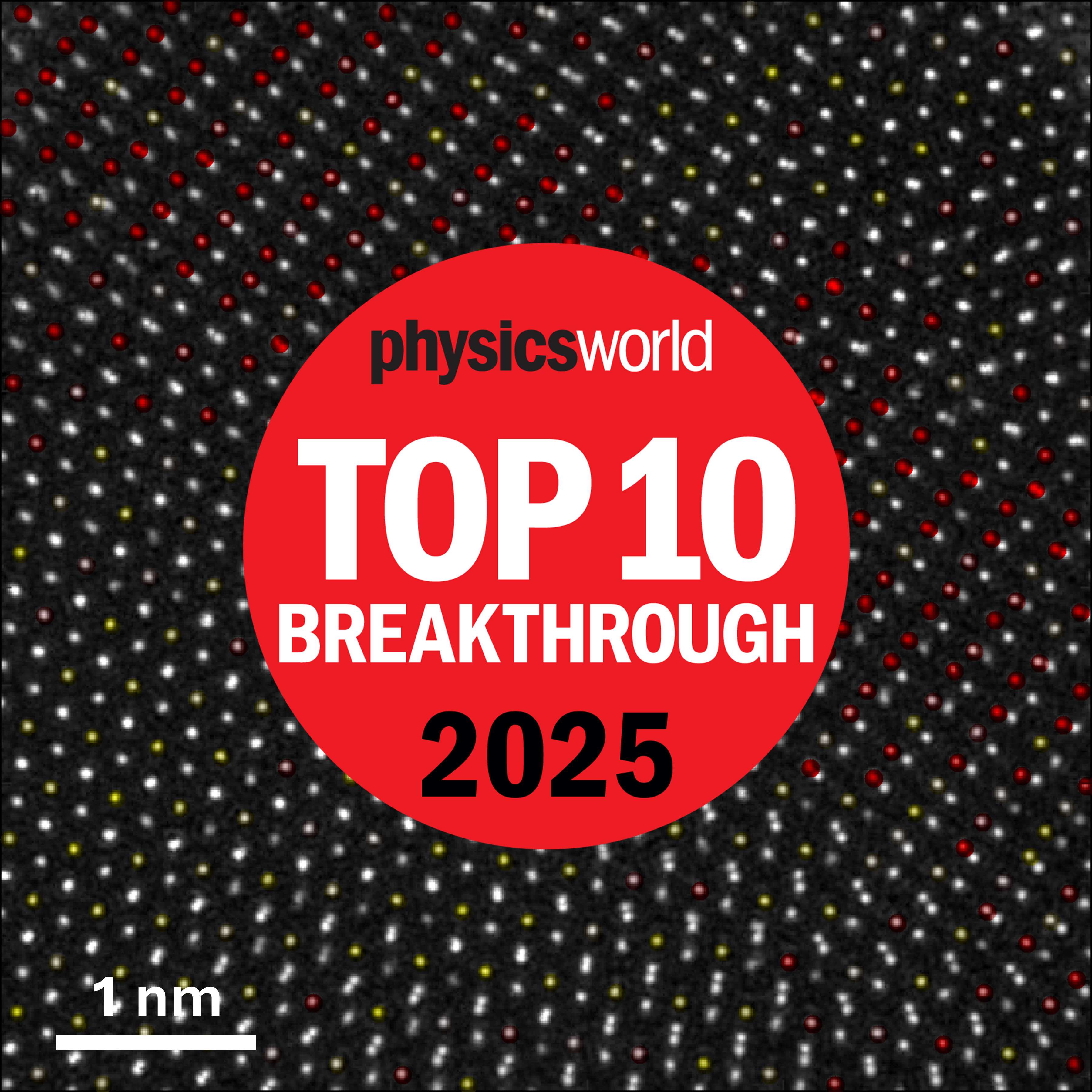
SiC is a semiconductor capable of operating at high temperatures, frequencies, and power. This makes it a good candidate for use in metal-oxide-semiconductor field-effect transistors (MOSFETs). However, it has been found that in MOSFETs fabricated with layers of SiC and silicon dioxide (SiO2), carbon atoms make their way into the SiO2, blurring the distinction between the two materials where they touch. Electrons move less efficiently through these muddied areas, resulting in a loss of energy and poor device performance.
"The high temperature at which devices made of silicon carbide operate causes the carbon to diffuse into the silicon dioxide," Salamanca-Riba explains. "Why exactly this happens is not well understood, but it's possible that it's because the two materials expand at different rates when as the temperature increases."
Salamanca-Riba and her colleagues were able to create a sharper interface between the layers of SiC and SiO2, as well as substantially increase performance, by treating the materials with nitrogen plasma in one experiment, and focused ion beam bombardment in another. The team is planning on testing two other possible treatments, annealing and ion implantation, in order to determine which yields the best results and could be implemented in the manufacturing process.
Published quarterly, CNST News reports on the latest developments in nanoscale fabrication, tool, processes, and measurement methods.
Download the Fall 2010 issue of CNST News (PDF) »
Published November 8, 2010


