News Story
Cumings Group Invents New Microscopy Technique
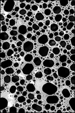
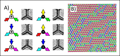
Indium islands deposited on a silicon nitride membrane. Each island serves as a binary thermometer, indicating its temperature based on whether it is solid or liquid, in a new imaging technique called electron thermal microscopy (ETM).
Often, Cumings explains, a nanoscale device or material is tested outside of the microscope, then put through an imaging process, creating "wait-time" and preventing researchers from receiving immediate feedback on their work. Cumings, however, envisions "a new future for the electron microscope as a fully-functional nano-laboratory." One of the ways he and his group are accomplishing this is through the use of the Nanoscale Imaging, Sprectroscopy and Properties (NISP) Lab's JEM 2100 LaB6 transmission electron microscope (TEM), coupled with video-rate imaging and special sample holders they have designed and constructed.
Devices for their experiments are fabricated in the FabLab, which, like the NISPLab, is part of the Maryland NanoCenter. The Cumings group starts with an electron transparent silicon nitride membrane only 100nm thick. "Islands" made out of indium (a metal similar to aluminum and zinc used in electronics) are then grown on the backside of membranes. The metal islands form an array of individual, binary thermometers, each reporting their local temperature as either above or below the melting temperature, 156.6°C. The Cumings group has demonstrated the technique using fabricated nanoscale heater wires. Different electrical currents conducted through the wires are used to generate heat, which in turn melts the islands. The melted islands comprise 'thermal maps' of the region. The resulting nanoscale maps agree with the group's theoretical models of temperature distribution, proving the utility of the technique.

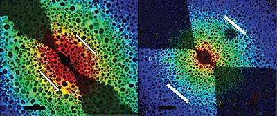
This figure shows a demonstration of the electron thermal microscopy technique. A patterned heater wire ~1 um long can be seen in part a as a straight line from bottom left to upper right, spanning two tapered electrodes which apply an electrical current to the wire (values on the far right). As the current increases, the islands melt, producing a binary temperature map where the temperature exceeds the melting point of 157°C. In b, each of these regions is assigned a color as shown on the far right, giving a thermal image of the temperature around the heater wire. In c, a theoretical model confirms the thermal microscopy results.
The ETM technique—one of the fastest, highest resolution, and most reliable for thermometry at this scale—will in the future be used to thermally characterize unknown nanosystems. This can be done through passive heating, in which heater wires are used to generate heat while unknown nanomaterials distort the temperature maps; or through active heating, in which the nanosystems themselves produce local heating when a voltage is applied to them. Active heating is extremely useful because both electrical and thermal conduction can be measured at the same time, while passive heating allows for electrical insulators to be measured. The technique is currently being used for thermal characterization of multi-walled carbon nanotubes.
For More Information:
1Brintlinger, T.; Qi, Y.; Baloch, K. H.; Goldhaber-Gordon, D.; Cumings, J. Electron Thermal Microscopy. Nano Lett.; (Letter); 2008; 8(2); 582-585. Abstract | Full Article (HTML)
Visit Professor Cumings' home page »
Related Story:
"New Microscopes for NISP, Keck Labs"
Published March 7, 2008
Related Stories
Stories / June 4, 2012
Cumings Promoted

Stories / August 18, 2010
Cumings Receives DOE Grant to Study Thermal Resistance of...
Stories / April 20, 2015
Nilsson Wins Wylie Fellowship
Stories / May 27, 2014
NSF Award Sponsors Student’s Microscopy Research in Sweden

Stories / April 9, 2012
The Weird World of "Remote Heating"
Stories / October 10, 2011
Cumings Wins Clark School's Junior Faculty Outstanding Research...

Stories / January 19, 2011
Cumings, Seog Win NSF CAREER Awards for Nanotechnology Research
Stories / December 22, 2010
Cumings Tapped for Nature Physics News and Views Column

Stories / November 11, 2010
NIST Awards NanoCenter $15 Million to Support Postdoc...
Stories / August 4, 2009
Cumings Leads EFRC Nanowire Team